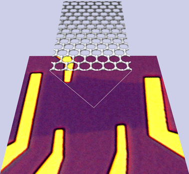
Graphene, a single two-dimensional sheet of graphite, has recently been realized experimentally. Graphene has an extremely unusual dispersion relation for electrons: the energy of electrons in graphene is linear in momentum, analogous to massless particles. This property leads to a number of differences between graphene and "ordinary" two-dimensional metals and semiconductors. Graphene devices are all surface area, and modifying the environment of graphene with adsorbates can be used to tune graphene's properties. Furthermore, graphene is ideal for scanned-probe studies, such as scanning tunneling microscopy, which can characterize the atomic lattice, electron wavefunctions, as well as defects and edges. We are studying the electronic properties of graphene in the Fuhrer group.
Fuhrer Group Graphene News:
"Is Graphene the New Silicon?" NSF Press Release, March 27, 2008.
"Carbon could enable fastest chips" by Colin Johnson, in EE Times, published online 25 March 2005.
"Physicists
Show Electrons Can Travel More Than 100 Times Faster in Graphene" UMD
Newsdesk release, March 24, 2008.
[see also stories at
slashdot.org,
tomshardware.com,
softpedia.com,
Scientific American Community, etc.]
"Graphene: What lies beneath" by Jessica Thomas, in Nature Nanotechnology, published online 25 May 2007.
Fuhrer Group publications on graphene:
“Diffusive Charge Transport in Graphene on SiO2,” J.-H. Chen, C. Jang, M. Ishigami, S. Xiao, E. D. Williams, and M. S. Fuhrer, to appear in Proceedings of Graphene Week 2008 Conference (arXiv:0812.2504)
“Tuning the effective fine structure constant in graphene: opposing effects of dielectric screening on short- and long-range potential scattering,” C. Jang, S. Adam, J.-H. Chen, E. D. Williams, S. Das Sarma, M. S. Fuhrer, Physical Review Letters 101, 146805 (2008) (download PDF) or (arXiv:0805.3780)
“Density inhomogeneity driven percolation metal-insulator transition and dimensional crossover in graphene nanoribbons,” S. Adam, S. Cho, M. S. Fuhrer, S. Das Sarma, Physical Review Letters 101, 046404 (2008). (download PDF) or (arXiv:0804.2253)
“Intrinsic and Extrinsic Performance Limits of Graphene Devices on SiO2,” J. H. Chen, C. Jang, S. Xiao, M. Ishigami, M. S. Fuhrer, Nature Nanotechnology 3, 206 - 209 (2008). (Nature Nanotechnology version) or (arXiv:0711.3646)
“Charged Impurity Scattering in Graphene,” J. H. Chen, C. Jang, M. S. Fuhrer, E. D. Williams, and M. Ishigami, Nature Physics, published online April 13, 2008. (arXiv:0708.2408)
“Printed Graphene Circuits,” Jian-Hao Chen, Masa Ishigami, Chaun Jang, Daniel R. Hines, Michael S. Fuhrer, and Ellen D. Williams, Advanced Materials 19, 3623 (2007). (available online at Advanced Materials)
“Gate-tunable Graphene Spin Valve,” Sungjae Cho, Yung-Fu Chen and Michael S. Fuhrer, Applied Physics Letters 91, 123105 (2007). (APL version) or (arXiv:0706.1597)
"Charge Transport and Inhomogeneity near the Minimum Conductivity Point in Graphene," Sungjae Cho and Michael S. Fuhrer, Physical Review B Rapid Communications 77, 084102(R) (2008). (download PDF) or (arXiv:0705.3239)
“Atomic Structure of Graphene on SiO2,” Masa Ishigami, J. H. Chen, W. G. Cullen, M. S. Fuhrer, and E. D. Williams, Nano Letters 7, 1643 (2007). (download PDF)
For further reading:
"Carbon Wonderland" by Andre K. Geim and Philip Kim, Scientific American, March, 2008.
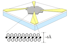
Nanopatches are small single-layer pieces of two-dimensional layered materials such as graphene (single layer of graphite) or niobium diselenide (NbSe2). We are working on techniques to synthesize these materials, following several routes. One method is to chemically disassemble these layered compounds into single-layer pieces in solution, and then deposit these pieces onto substrates. Another technique is to grow these materials directly on substrates, taking advantage of their propensity to self-assemble into layers.
These nanopatches will act as two-dimensional boxes for electrons, and the electron interaction may be tuned widely by varying the materials used to form the nanopatch: graphite is a low-electron-density semimetal, while the dichalcogenides may be metallic (ex: NbSe2, TaS2) or semiconducting (ex: MoS2), and exhibit charge-density wave and superconducting phases. In addition, the electron density in the patch may be tuned significantly by using a backing electrode as a field-effect gate. The electronic properties of nanopatches can be probed using scanned probe techniques such as STM and scanned-gate microscopy, as well as through electronic transport via lithographically-defined metal leads.
 |
 |
|
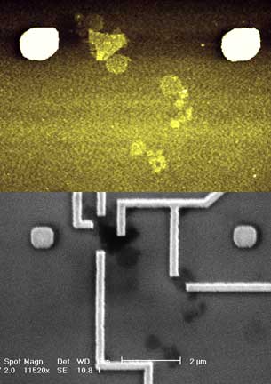
| Schematic of a nanopatch. The nanopatch (grey) consists of a single three-atom-thick layer of a transistion metal dichalcogenide compound (black circles are transition metal, e.g. Ta, Mo, Nb; open circles are chalcogen, e.g. S, Se). | The top image is an atomic force micrograph of MoS2 nanopatches on an SiO2 surface. The large squares are alignment markers used to locate the patches. These patches are 3-6 layers thick. The bottom image shows a scanning electron micrograph of the nanopatches contacted with gold electrodes. |
Fuhrer Group publications on other nanopatches:
“Realization and electrical characterization of ultrathin crystals of layered transition-metal dichalcogenides,” Anthony Ayari, Enrique Cobas, Ololade Ogundadegbe, and Michael S. Fuhrer, Journal of Applied Physics 101, 014507 (2007). (download PDF)